- Stok Durumu: Stok Var
- Marka: WINBOND
- SKU: RBZ.100.815
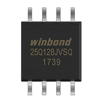
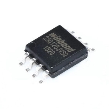
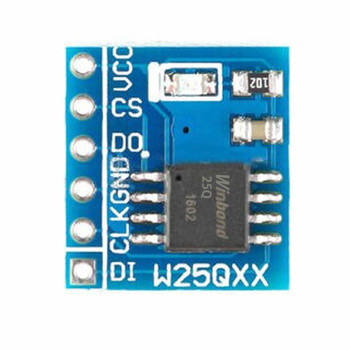
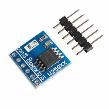
Winbond W25Q64JVSIQ 64M-bit Serial Flash 3.3V SPI
Memory IC 32768 Page Uniform 4KB Sector SOP8 Wide 208mil Package Quad I/O 64-Bit Unique ID
The W25Q64JVSIQ is a 64M-bit (8MB) serial NOR flash memory IC from Winbond's W25Q64JV series. It runs from a single 2.7V - 3.6V supply (3.3V), supports standard SPI, Dual SPI and Quad SPI interfaces, and the clock frequency goes up to 133MHz. The memory consists of 32768 pages of 256 bytes; it can be erased in 4KB sectors, 32KB and 64KB blocks or as a whole chip.
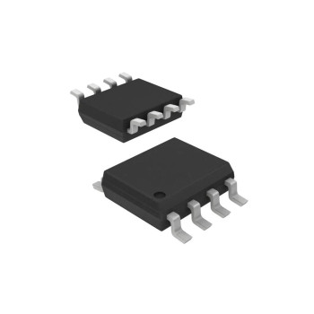
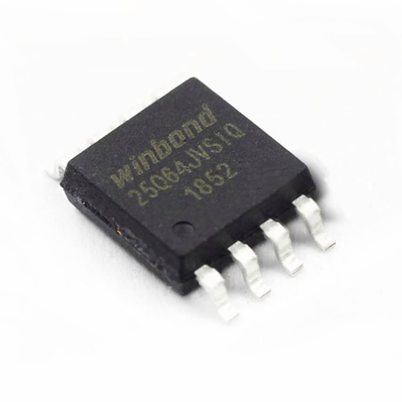
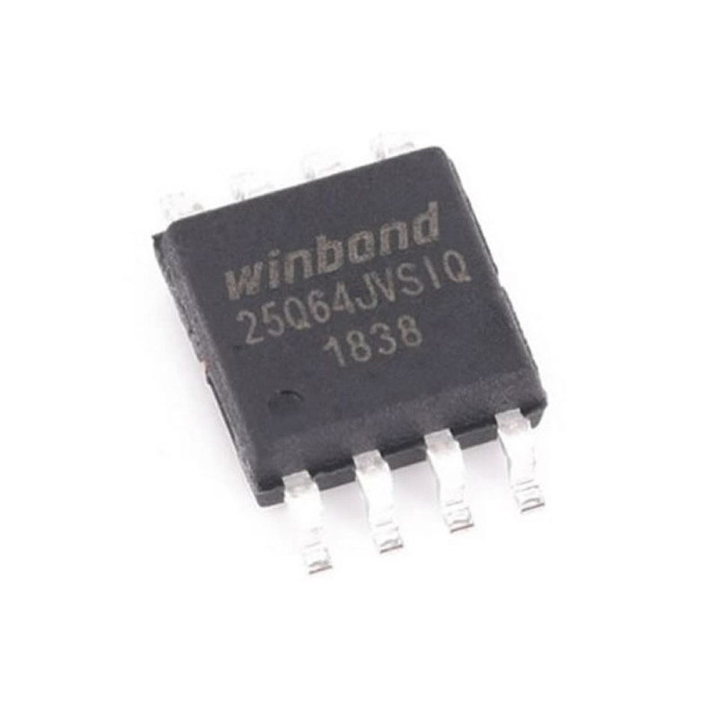
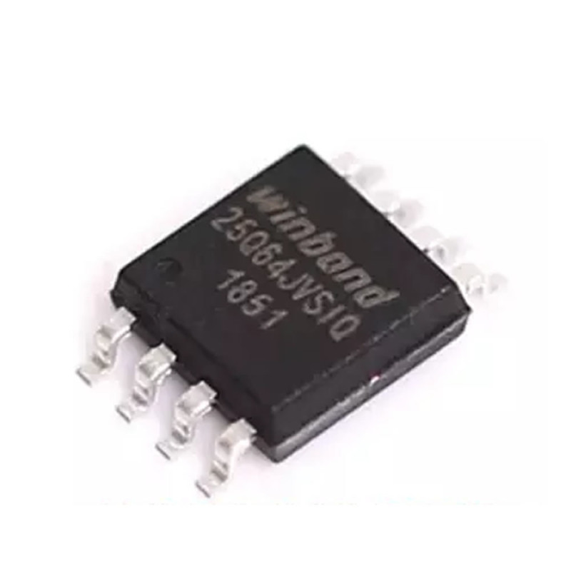
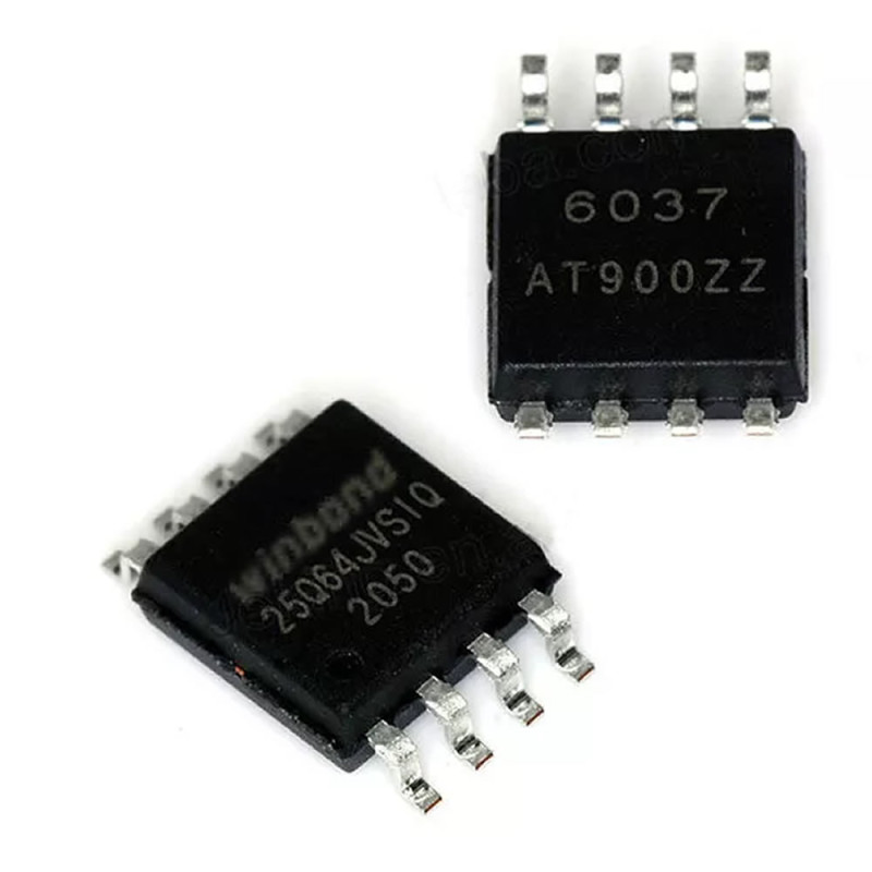
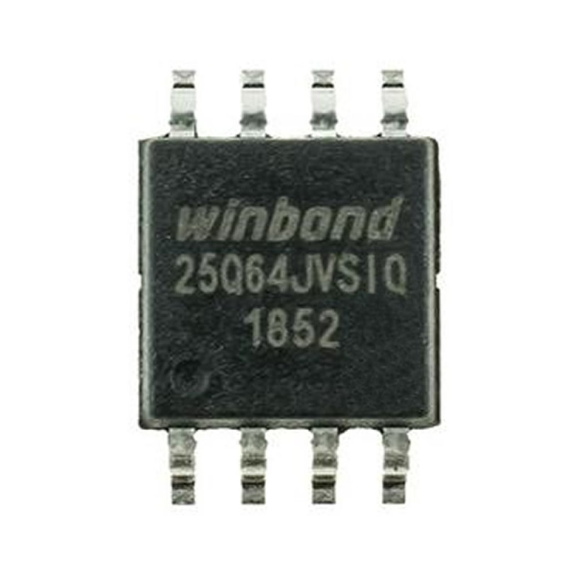
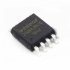
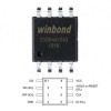
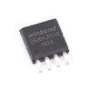
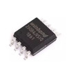
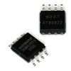
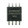
The IC comes in an 8 pin, wide body SOIC-8 (SOP8, 208mil) package; the top is marked "winbond 25Q64JVSIQ" with a date code. According to the manufacturer it offers a minimum of 100,000 program/erase cycles per sector and more than 20 years of data retention; in power-down mode it draws typically below 1µA. It operates over the -40°C - +85°C industrial temperature range.
It is used to replace motherboard and laptop BIOS chips, to renew the 64M-bit SPI flash memory on router, modem, satellite receiver and TV boards, and to store firmware, data logs or font / image data on your own boards. Values are from the Winbond W25Q64JV datasheet.
Key features:
8MB capacity, 4KB sectors: The 64M-bit memory is split into 32768 pages of 256 bytes. 4KB sector erase lets small pieces of data be updated without erasing a whole block.
133MHz Quad SPI: Standard, Dual and Quad SPI reads are supported; in Quad mode a 133MHz clock gives 532MHz equivalent speed. In this version (IQ) the Quad Enable bit (QE) is fixed to 1 at the factory, so Quad reads need no setup.
Long life: At least 100,000 program/erase cycles per sector and more than 20 years of data retention; suitable for frequently updated settings and log data.
Low power consumption: Draws typically below 1µA in power-down mode, keeping standby consumption low in battery powered devices.
Security and protection: Each IC has a 64-bit unique ID, 3 lockable 256 byte security registers and block write protection through the status register bits.
Features:
- Product type: Serial NOR flash memory IC (SPI)
- Manufacturer / model: Winbond W25Q64JVSIQ (W25Q64JV series)
- Capacity: 64M-bit (8MB), 8M x 8 organisation
- Interface: Standard SPI, Dual SPI, Quad SPI (Quad I/O)
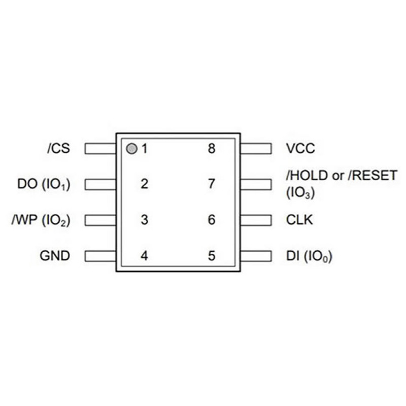
- Quad Enable bit: QE=1 fixed at the factory (IQ version); pin 3 and pin 7 are IO2 / IO3, no /HOLD function
- Clock frequency: Up to 133MHz
- Read speed: Dual 266MHz, Quad 532MHz equivalent clock
- Supply voltage: 2.7V - 3.6V (3.3V)
- Page structure: 32768 pages x 256 bytes
- Erase units: 4KB sector (2048 sectors), 32KB block, 64KB block (128 blocks), full chip
- Page program time: 0.8ms typical, 3ms max
- 64KB block erase time: 150ms typical, 2000ms max
- Endurance: Minimum 100,000 program/erase cycles per sector
- Data retention: More than 20 years
- Current: Power-down 1µA typical (15µA max), standby 10µA typical (50µA max), read 20mA max (104MHz), program / erase 25mA max
- Security: 64-bit unique ID, 3 x 256 byte lockable (OTP) security registers, SFDP table
- Write protection: Software and block protection (BP, TB, CMP bits); the /WP pin locks the status register during Standard / Dual SPI operations
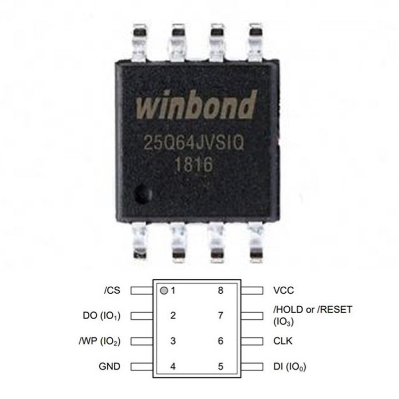
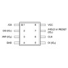
- Pinout: 1 /CS, 2 DO (IO1), 3 /WP (IO2), 4 GND, 5 DI (IO0), 6 CLK, 7 IO3 (/HOLD), 8 VCC
- Memory technology: NOR flash, moisture sensitive package
- Operating temperature: -40°C - +85°C
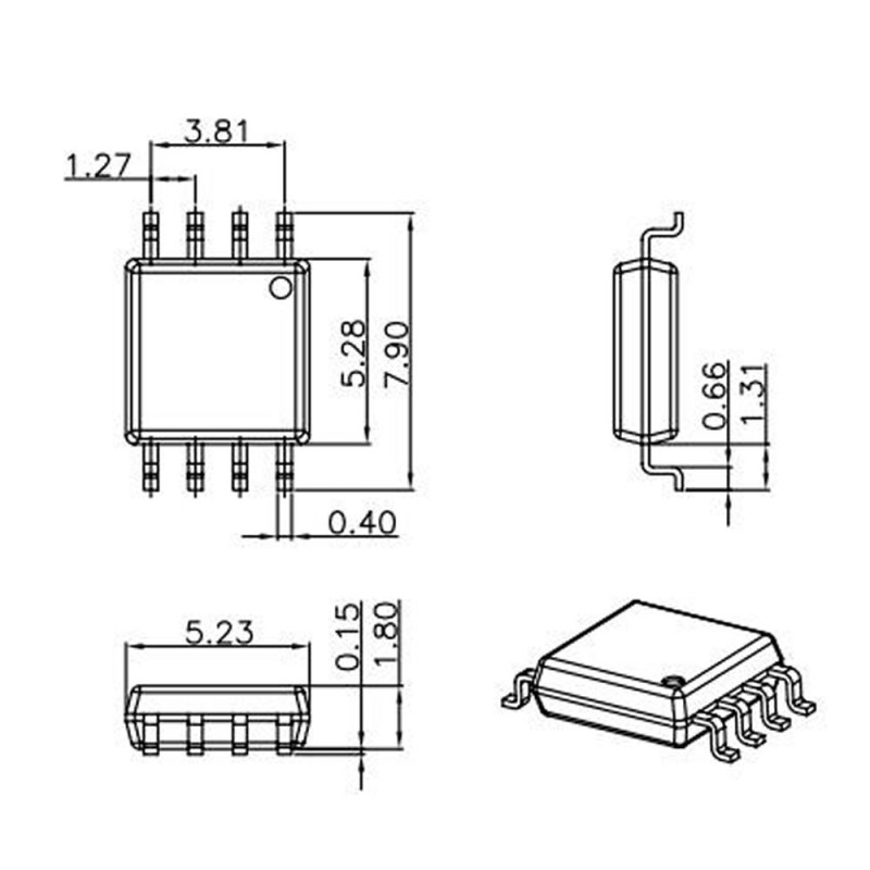
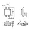
- Package: SOIC-8 (SOP8) wide body 208mil (5.30mm body width), 1.27mm pin pitch, surface mount
- Top marking: winbond 25Q64JVSIQ + date code
- Weight: Below 1gr
Usage information:
- Solder the IC onto a 208mil (wide) SOIC-8 footprint with the pin 1 dot on the body matching the pin 1 mark on the board. Pin 8 is VCC (3.3V), pin 4 is GND; place a 100nF decoupling capacitor between VCC and GND close to the IC.
- For standard SPI, connect pin 1 /CS, pin 6 CLK, pin 5 DI and pin 2 DO to the SPI pins of the controller; do not leave pin 3 (IO2) and pin 7 (IO3) floating, pull them up to VCC. In this version QE=1 is fixed, so these two pins are always the IO2 / IO3 data lines; the /HOLD function cannot be used.
- When replacing BIOS or device firmware, first read and back up the old chip content with an SPI programmer (CH341A etc.), then write it to this IC and run a verify.
Application areas:
- Motherboard and laptop BIOS / UEFI chip replacement and repair (64M-bit sockets)
- Router and modem firmware memory
- Satellite receiver and TV main board firmware memory
- Printer and office equipment board repair
- External data and log memory in microcontroller circuits
- Font and image data storage in display circuits
- FPGA configuration memory
- Firmware and settings storage on your own boards
- Audio file storage in sound player circuits
Precautions:
- The supply range is 2.7V - 3.6V. Do not power the IC from 5V; connect it to a 5V logic controller through a level shifter.
- The package is a 208mil wide body; it does not fit a 150mil narrow SOIC-8 footprint properly. Before replacement, check the body width and capacity (64M-bit) of the old chip on the board.
- The IC does not contain any BIOS or device firmware; you need to load the firmware yourself.
- This version has no /HOLD function (QE=1 fixed). If your circuit uses the /HOLD pin, the W25Q64JVSSIM version with a settable QE bit is needed.
- It is sensitive to static electricity; use a grounded wrist strap and a grounded soldering iron. The package is moisture sensitive; store opened ICs in a dry place.
- In flash memory the sector must be erased before writing; data written to an unerased area reads back corrupted.
Package contents:
- 1 Piece Winbond W25Q64JVSIQ 64M-bit Serial Flash
- Note: Programmer and adapter are not included in the package.